- MIPI CSI-2 receiver and decoding block
- Configurable number of MIPI Lanes
- Using AMD D-PHY IP
- Delivered as working reference design for fast development
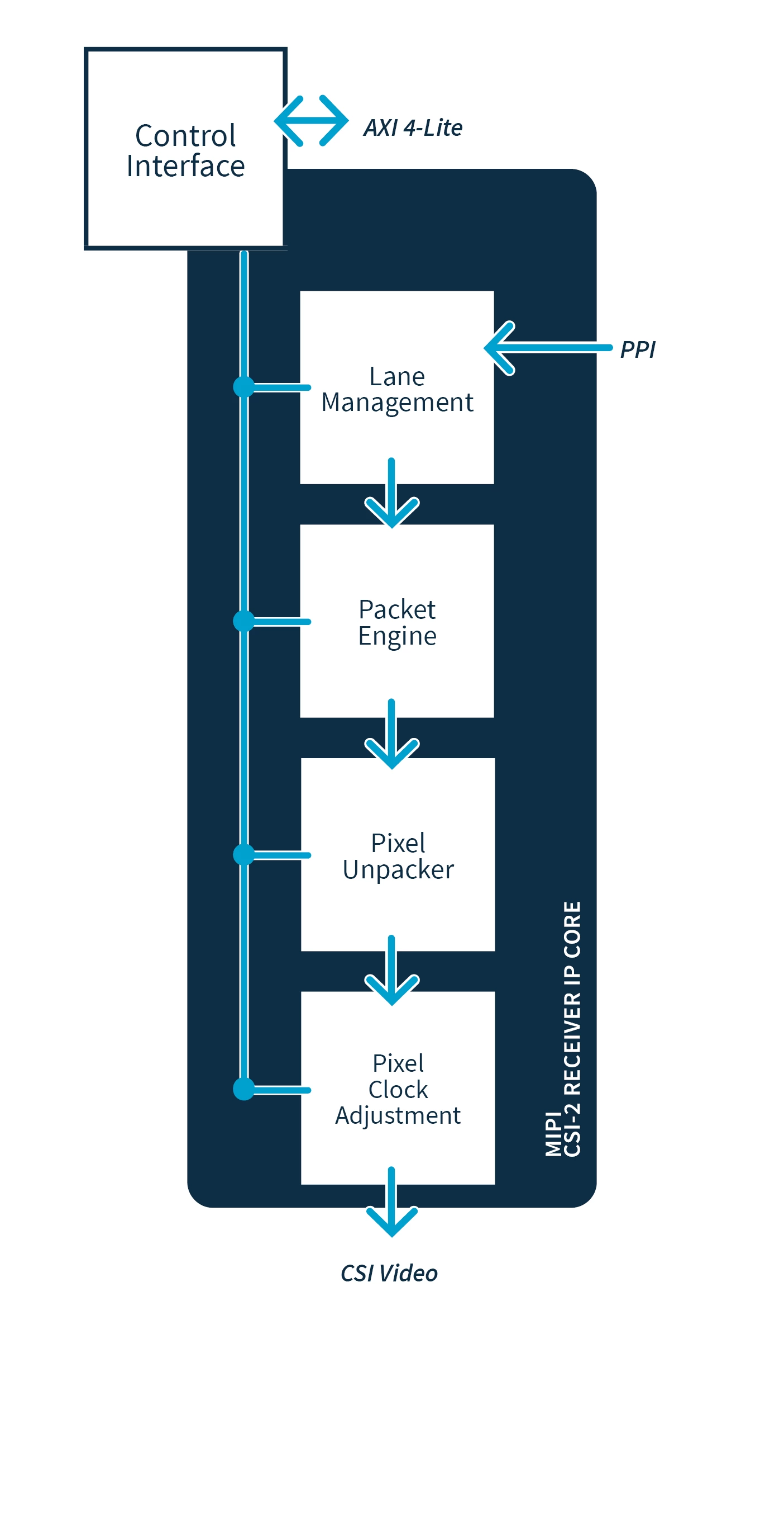
Architecture
Image sensors with MIPI interface are not only used in mobile phones, but also in industrial and automotive applications. These applications often require an FPGA for control and further processing. This IP helps to interface MIPI sensors of different vendors to FPGAs. The IP relies on an existing D-PHY implementation, typically available from FPGA vendors. The IP is delivered as a fully functioning reference design that is running on an agreed common delivey platform along with a MIPI FMC module compatible with S2I’s MVDK and standard FPGA evaluation kits. Together, they provide an easy way to design a camera.
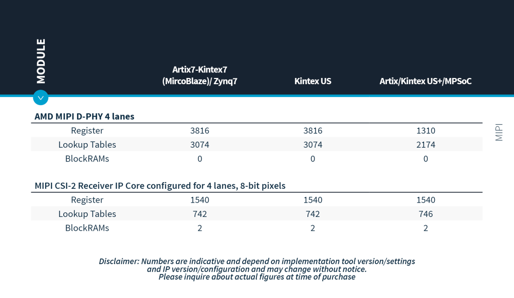
Resource Usage
Download resource usageBenefits
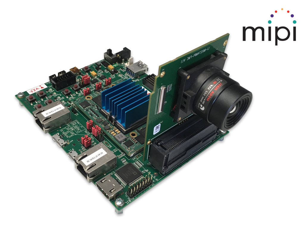
MVDK With MIPI CSI-2 Interface Board
Main Features
- FPGA technology independent
- PPI interface to connect to different D-PHY implementations
- Configurable to 1, 2 or 4 data lanes
- Any lane rate (limited by the used FPGA)
- RAW8, RAW10, RAW12, RAW14, RAW16 standard MIPI data types
- Embedded data decoding
- Direct output of reordered byte stream without pixel unpacking
- AXI4-Lite slave control interface
Delivery
The IP Core is delivered with a complete reference design for S2I’s MVDK with a Zynq7 or Ultrascale+ FPGA and an IMX MIPI FMC module. Since the physical interface is abstracted by the AMD D-PHY core, it is easy to port the design to other FPGA platforms like, for example, the 7 series AMD FPGAs.
Modules Available
The MIPI CSI-2 Receiver IP Core is delivered as encrypted VHDL. It is optionally available as VHDL source code. It is compatible with AMD Artix7, Kintex7, Zynq7 and Ultrascale+ FPGAs. The MIPI CSI-2 Receiver IP Software library is delivered as an object file. It is optionally available as C source code.